Research
1. Soft Nanoimprint Lithography
There is a need for a new generation of light management systems to suit the needs of emerging optoelectronic devices where the development of new large area and low cost fabrication routes can considerably reduce the manufacturing costs and increase the production throughput.
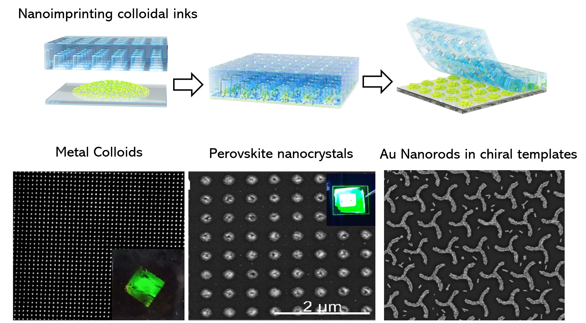
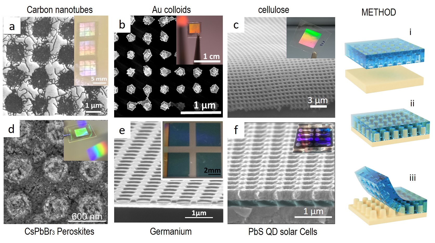
Soft nanoimprint lithography is a promising approach for satisfaying all these requests. This unconventional nanofabrication technique enables the creation of photonic and plasmonic architectures based on unconventional materials such as colloids, polymers, cellulose and many others. We combine the intrinsic properties of the materials with the complex optical response given by the nanostructuration.

2. Cellulose-based photonic architectures
Pollution and environmental degradation are a source of strong concern in nowadays societies. In order to minimize it, there exist a huge demand for new ecofriendly materials able to replace standard ones. Cellulose and its derivatives have gained renewed interest as favorable alternatives to traditional plastics due to their abundance and lower environmental impact. In our group we explore the development of new and less enviromentally agressive fabrication methods as well as their application in photonic and plasmonic systems based on green cellulose.

3. Template-assisted self-assembly
Metal colloids are of great interest in nanophotonics mainly due to their morphology-dependent optical properties but also because they are high quality building blocks for the fabrication of complex plasmonic architectures. Making use of template-assisted self-assembly, we create hierarchical plasmonic arrays that exhibit well-defined collective plasmon modes from the visible to the NIR. Our approach along with the strong local confinement of the electromagnetic field make our structures highly efficient, uniform and reproducible substrates sustaing high Q factor resonances for lasing, SERS sensing and even chirality.

4. Metamaterials and metasurfaces
Despite the exciting optical properties metamaterials and metasurfaces exhibit, their implementation in current optoelectronic devices is being hampered by the expensive and low-throughput used procedures. Nanoimprint and colloidal lithography stand out in nowadays nanotechnology for being low cost and scalable approaches. The proper control and combination of materials and nanostructures allows the achievement of tunable index metamaterials as well as high dielectric superabsorbers from the visible to the NIR.

5. Light trapping in photovoltaic systems
The prospect of an efficient clean energy source and the need of converging light speed data transfer with current electronics push the scientific community into developing more economic and effective ways to convert light into active electrons. Light trapping is a promising strategy for enhancing light matter interaction in optoelectronic devices. By nanostructuring the active layer, we can improve the absorption efficiency of devices such as quantum-dot solar cells with no deterioration of the electronic properties.

6. NIL is compatible with a variety of materials and properties
